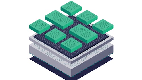
Reduce 3D IC design complexity with early package assembly verification

As 2.5D and 3D ICs redefine the possibilities of semiconductor design, the Calibre Shift Left solutions address the challenges of physical verification. By automating the verification of each chiplet against its foundry process and streamlining full assembly verification, we significantly reduce the risk of human error and the time-consuming task of managing multiple rule decks.
Introducing Calibre Shift Left, a revolutionary solution from Siemens EDA
- Reduce debugging efforts. Identify and address issues earlier in the design flow.
- Focus on what matters most. Utilize the power of post-assembly netlist generation for comprehensive verification.
- Ensure design integrity. Multi-physics analysis ensures that electrical behaviors are accurately predicted and mechanical stresses are meticulously accounted for.
- Improve productivity. Automate the integration of design-specific data for efficiency and accuracy.
Ready to learn how Calibre Shift Left solutions can boost productivity for 2.5D and 3D IC designs? Download the full technical paper to learn more about Calibre Shift Left and how it can transform your verification workflow.
